Table of Contents
68k-MBC
Description
The 68k-MBC is an easy to build 68008 CPU SBC (Single Board Computer), using only easy to find TH parts.
It follows the same “concept” of the previous Z80-MBC2 and V20-MBC boards, using a PIC18F47Q10 MCU as EEPROM and “universal” I/O emulator (so a “legacy” EPROM programmer is not needed).
You can choose between two main HW configuration options: Lite or Full.
Lite HW configuration option allows to build a 3 ICs 68008 system running CP/M-68K.
It has an optional on board 16x GPIO expander, and uses common cheap add-on modules for the SD (HD emulation) and the RTC options.
Having two onboard RS232 serial ports, it allows to connect RS232 terminals like uTerm-S.
It is compatible with the uTerm and uCom add-on boards.
Details
PROJECT STATUS (01/07/2021)
HW:
- Released all the HW related files (see the FILES section);
SW:
- Released all the SW related files (see the FILES section);
- Updated IOS S310121-R130421 and SD-S310121-R130421-v1.zip (see the FILES section);
- Added the complete collection of the 4 Manuals of CP/M-68K (see the FILES section);
- Updated IOS S310121-R150421 and SD-S310121-R150421-v1.zip (see the FILES section);
- Added the SW/FW for the Arduino Uno PIC programmer, including the “ICSP Shield” board (see the paragraph:
- FLASHING THE FIRMWARE WITH AN ARDUINO UNO AS PROGRAMMER);
- Updated SD-S310121-R150421-v2.zip (see the FILES section);
- Released a working experimental doker image for a gcc cross-compiler toolchain (See the paragraph: SLOAD:
- HOW SETUP A “DOCKERIZED” GCC + NEWLIB CROSS-COMPILING AUTOMATED TOOLCHAIN (LINUX));
- Updated IOS S310121-R250521 and SD-S310121-R250521-v1.zip (see the FILES section);
- Added the 68000 IDE installation files and the custom cstart.asm file for the 68k-MBC (128/512/1024KB versions. See the FILES section);
- Updated SD-S310121-R250521-v2.zip (see the FILES section);
- Updated IOS S310121-R010721 and SD-S310121-R010721-v1.zip (see the FILES section).
DOCS:
- Task in progress…
The Prototype
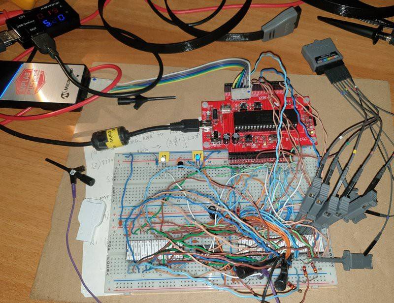
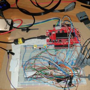
In the first phase of the design I've used a prototype on a breadboard to check the basic “concepts”.
I've used as “companion” MCU a PIC18F47Q10 on a custom board (PicOne) I previously made and that it is directly pluggable on breadboards, and with onboard microSD card and USB-serial adapter.:
To make the firmware for the PIC18F47Q10 I've used MPLAB X IDE with the MMC plugin.
Here a short video with an automated assembler toolchain using Easy68K as assembler and sLoad, a custom SW utility to load from the serial port and execute a Motorola S-record formatted executable:
To allow a real automated toolchain an auto-reset circuit on the breadboard takes the DTR signal from the serial-USB adapter and uses it to reset the MCU (like in the Arduino Uno board), so it is possible reset the breadboard from a batch file running in the PC using a macro of Tera Term.
Why a PIC ?
Those have followed the previous Z80-MBC2 and V20-MBC boards will note that I haven’t used here an Atmega MCU.
Using an Atmega MCU allows to use the friendly Arduino IDE and many ways to flash the MCU, so this is an enabling factor.
Unfortunately Atmega MCU GPIO ports are not TTL compatible, and this limitation was solved in the previous boards using a CMOS CPU that under given conditions can accomplish the digital levels of the Atmega MCU.
But here the 68008 CPU isn’t available in CMOS technology at all, so an Atmega MCU cannot be used.
So I’ve done some searches to find an alternative MCU having three main constraints: must have TTL compatible GPIOs (I mean strictly “guaranteed” TTL compatible), must be a TH part and cheap too.
The only part I’ve found was a PIC18F47Q10 MCU, and I must say that it accomplish the previous constrains very well. More, it is a modern MCU with lot of interesting features and more flash and RAM memory than the previous Atmega32 MCU.
Of course nothing comes free, and the choice of a PIC18F47Q10 brings some complexities.
The first is the need for an appropriate HW programmer to perform the flashing (however I've found a way to use a common Arduino Uno board as PIC programmer.
See the paragraph “FLASHING THE FIRMWARE WITH AN ARDUINO UNO AS PROGRAMMER” below).
The second is the constraint to use a proprietary IDE (MPLAB X) to write or modify the source that is more complex to use than the Arduino IDE (but I must say a lot more powerful…).
Those wanting make modifications to the firmware will have to install the MPLAB X IDE and learn to use it.
MPLAB X is a professional tool, and with a lot of “power” comes a lot of complexity too…
I hope this won’t be a problem, and after all learn to use a professional tool like MPLAB X IDE is always a good thing.
Hardware overview
Here the 68k-MBC hardware main specs:
- 68008 CPU running at 8MHz;
- multi-boot capability;
- two main HW configuration options: Lite or Full. Lite HW configuration option allows to build a minimal 3 ICs 68008 system;
- RAM can be configured as 128/512/1024KB (1024KB supported on the Full HW configuration option only);
- optional RTC and microSD (HD emulation) modules (the same used in the Z80-MBC2);
- optional 16x GPIO port;
- I2C expansion port;
- 2 serial ports (Serial Port 2 supported on the Full HW configuration option only);
- on board RS232 drivers for both the two serial ports (Full HW configuration option only);
- serial-USB adapter support on the Serial Port 2 with independent power supply (Full HW configuration option only);
- User led and key;
- ICSP connector (for the PIC18F47Q10) for an easy firmware installation/upgrade;
LITE/FULL HW configuration options
The 68k-MBC allows to choose between two main HW configuration options: Lite or Full.
Lite HW configuration allows to build a minimal 3 ICs 68008 system running CP/M-68K.
The two HW configurations are quite different, and some signals behave in a complementary way. The IOS firmware checks which one HW configuration is used at first and changes the signals behavior accordingly (where needed).
The Lite HW configuration need less components populated than the Full one, with the only exception of one resistor (R4) that is needed only for the Lite HW configuration and is not needed with the Full HW configuration (anyway it will not “hurt” if present on the Full HW configuration).
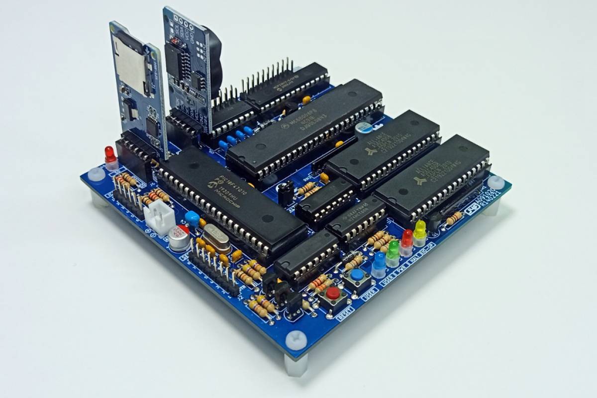
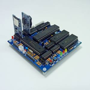
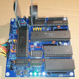
The following photo shows the 68k-MBC with the Lite HW configuration populated:
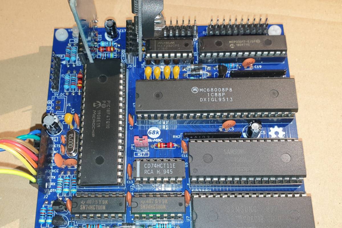
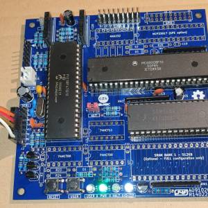
The following photo shows the 68k-MBC with the Full HW configuration populated (previous PCB revision):
To simplify the selection of the components a modular BOM shows the components needed for the two HW configurations.
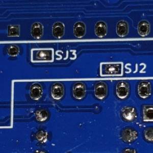
An important task to do at first is the configuration of the three solder jumpers (SJ1, SJ2, SJ3) on the bottom side of the PCB.
After you have chosen the wanted HW configuration to implement you must set the three solder jumpers SJ1, SJ2 and SJ3 in the following way:
- If you have chosen the Full HW configuration just leave all the three jumpers open;
- If you have chosen the Lite HW configuration all the three jumpers must be shorted.
WARNING: Permanent damages may occur if you don't follow the previous procedure as described!
WARNING: Permanent damages may occur if the three jumpers are shorted when U1, U2 and U5 are populated!
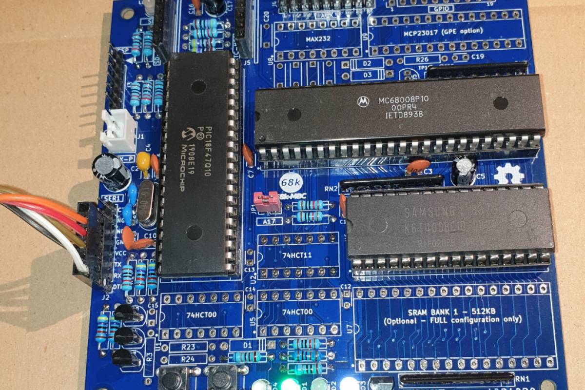
In the following photo SJ1, SJ2, and SJ3 are all shorted to enable the Lite HW configuration:
Limitations of the Lite HW configuration option
The Lite HW configuration option allows to build a 68008 system with a minimal BOM, but brings some limitations compared with the Full one:
- the 1024KB RAM configuration is not supported. Only 128/512KB are allowed;
- in the AUX connector only the I2C port is present;
- only the Serial Port 1 can be used (at the SER1 connector only);
- is not possible to use the CPU interrupts.
Anyway it can run all the provided SW, CP/M-68K included.
RAM configuration
The supported RAM configurations are different for the two Lite/Full HW options.
The Full HW option allows three different RAM configurations:
- 128KB (1x128KB);
- 512KB (1x512KB);
- 1024KB (2x512KB).
To set the 128KB RAM configuration the JP1 jumper (A17) must be left open, while to set the 512KB or the 1024KB configuration JP1 must be closed.
This operation must be done when the board is not powered, and before the first power on with the RAM chips installed.
Please note that only a single RAM chip configuration is allowed when using 128KB RAM (2x128KB is not supported).
The Lite HW option supports 128KB and 512KB only, setting JP1 as for the Full one (the 1024KB RAM configuration is not supported for the Lite HW option).
The GPE option
It is possible to choose to populate on the PCB a GPIO port expander to add 16 bidirectional GPIO pins.
The GPE option (see the schematic) can be used with both the Lite and Full HW configurations.
The modular BOM shows the components needed for the GPE option enabled.
Address space for the Full HW configuration option
The Full HW configuration uses a 16KB I/O address space (decoding A14-A19 with the three gates U2A, U2B and U5A) while the remaining 1008KB are left for the RAM address space.
This seemed to me a good tradeoff between needed HW to implement it and “wasted” RAM address space.
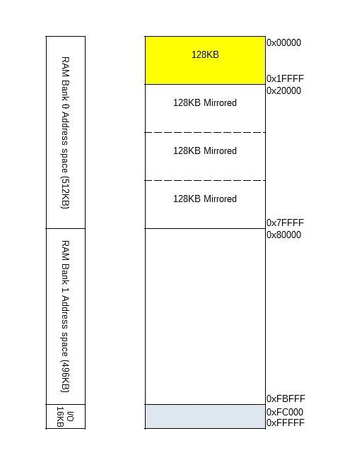
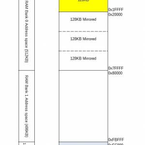
128KB RAM configuration.
When using a 128KB RAM the remaining address space inside the Bank 0 is “mirrored” into the first 128KB address block:
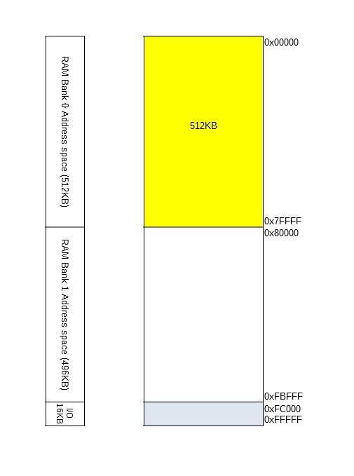
512KB RAM configuration.
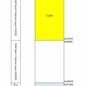
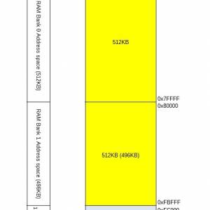
When using a 512KB RAM all the Bank 0 address space is used as shown in the following table:
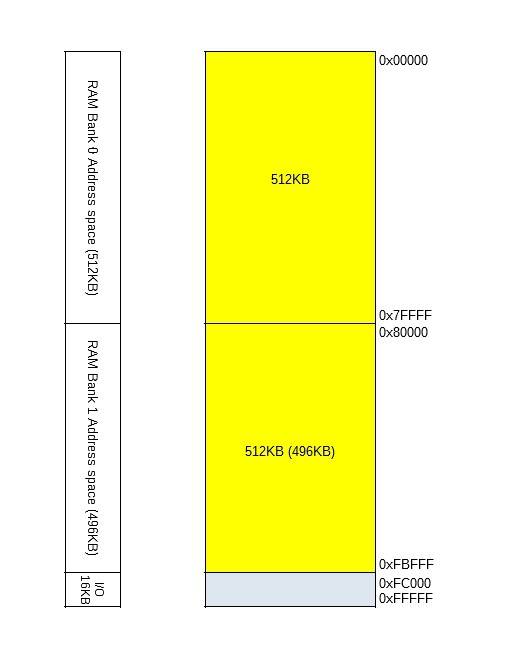
1024KB RAM configuration.
When using a 1024KB RAM the real RAM addressable space is only 1008KB because 16KB are “taken” from the Bank 1 for I/O:
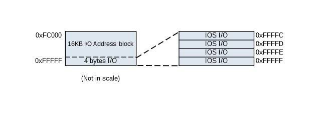
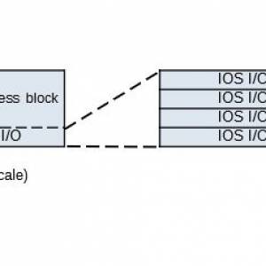
The address space for all the 128/512/1024/KB configurations is always 16KB wide (from 0xFC000 to 0xFFFFF), but only 4 bytes are really used (from 0xFFFFC to 0xFFFFF):
How to get a PCB
I've prepared an “easy link” to order a small lot (min. 5 pcs) of PCB here.
How to get a Kit or an Assembled unit
If you are looking for a kit with all the needed parts (including the 3D printed parts) or an assembled unit ready to use there is a professional seller that can sell both and ship worldwide.
The link to the seller is this one.
68k-MBC User Group
An “User Group” was created on Facebook (it is the same used for the Z80-MBC2).
Credits & License
All the project files are licensed under GPL v3.
Files
Schematic.
A091020-R140221-SCH.pdf.
BOM file.
A091020-R140221_v3.ods.
PCB Gerber files (100mm x 53mm).
A091020-R140221_Gerber.zip.
PCB Assembling Guide.
A091020-R1402219_Assembling_Guide.zip.
The sources for the IOS (with the needed libraries).
Unzip into a folder and open with MPLAB X IDE (I've used version v5.45).
IOS must be uploaded into the PIC18F47Q10 flash.
See the CHANGELOG section on main.c source for more info on changes.
S310121-R010721_68k-MBC_IOS.X.zip.
The IOS in executable format (.HEX).
This executable file is intended for the use with MPLAB IPE (or any other equivalent SW) to program the PIC MCU directly.
S310121-R010721_68k-MBC_IOS.X.production.hex.zip.
The content of the microSD for IOS S310121-R010721.
Added the /gcc-68k folder with the gcc cross-compiler related files.
See the CHANGELOG.TXT file inside the SD root for more info on changes.
SD-S310121-R010721-v1.zip.
68000 IDE installation files.
Unzip into a folder and run SETUP.EXE to install the 68000 IDE on your Windows system.
ide68k30.zip.
PIC programmer using an Arduino Uno.
All the needed SW/FW with my changes already applied, and all the documentation of the “ICSP Shield” board (A170421).
Arduino_Uno_PIC_programmer.zip.
The schematic of the RS232 AUX cable.
A020221-AUX_RS232_Cable.pdf.
The complete collection of the 4 Manuals of CP/M-68K.
CPM-68k_Manuals.zip.

